 Fraunhofer Group for Materials and Components - Materials
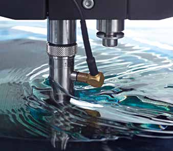
In order to increase the package density and performance of microelectronic components, many manufacturers extend the architecture to the third dimension with stacked chip setups. These novel component architectures that contain newly developed interconnection technologies entail enormous technical challenges along the production chain. A number of new failure mechanisms must be investigated and clarified. A group at the Fraunhofer Institute for Microstructure of Materials and Systems IMWS in Halle has specialized in this area and in the development of sophisticated analysis techniques and equipment.
Scanning acoustic microscopy is a non-destructive technique and plays an important role in defect detection and failure analysis. Together with the appliance manufacturer PVA Tepla Analytical Systems GmbH, Fraunhofer IMWS has developed a new, internationally unique, acoustic microscope in the ultrahigh-frequency range of up to 2 GHz.
The capability of defect analysis in thin layer systems, the metrological acquisition of mechanical parameters as well as a very high lateral resolution and sub-surface sensitivity in single-digit micrometer areas open up new fields of application for acoustic microscopy. In collaboration with the Belgian research center IMEC, the recently developed GHz ultrasound microscope was successfully used for the verification and localization of defects in innovative 3D contacting microelectronic chips: Through Silicon Vias (TSV). Together with PVA Tepla as well as additional partners from the industry and Fraunhofer, further areas of application will be opened up in the future for the method that PVA Tepla introduced onto the market in 2014.